soldering and desoldering of various components
INTRODUCTION
SOLDERING PROCESS:

Soldering is the process of joining two or more metals at temperature below there melting points using filler metal (solder) having melting point below 450`c. The solder binds the metal together by chemical & physical processes. Chemically solder reacts with small part of each metal to be joined or soldered, thus forming a new compound. Physically the liquid solder alloy then enters the exposed pores of the metals. Solder on cooling solidifies and forms a continuous metallic bond. If the metals are not heated properly, solder will not penetrate into the metal pores. As a result solder will solidify over the top of the pores in the metal & this result in defective joint known as cold solder joint
SOLDER :
Most of the soldering in electronics is done using tin lead alloy. Pure lead melts at 327`c where as tin melts at 232`c and their mixture at 188`c when ratio of tin & lead is 60/40.
The tin lead ratio at which the solder alloy goes directly to liquid stage is called ELECTRNONIC COMPOISITION & resultant alloy is known as EUTECTIC ALLOY. This alloy is generally referred to as 63/37 .The addition of antimony to this alloy increases the strength. The tin lead alloy is drawn into hollow wire whose centre is fixed with flux. This is known as ROSIN CORE SOLDER. For general soldering 18 gauge wire solder is used.
FLUXES:

A flux should have the following properties:
1 It must be sufficiently active at room temperature to remove oxides.
2 It must be mobile enough to allow the solder to flow at this temperature.
3 It must remove fingerprints, dirt, grease etc.
Traditionally fluxes can be grouped as:
1. Rosin based fluxes.
2. Water soluble fluxes.
3. Solvent removable synthetic fluxes.
4. Low solid fluxes.
Of these rosin based fluxes are generally used for repair work. These consist of rosin dissolved in some solvent.
TINNING:
The component leads may get rusted during storage. It will be difficult t solder such leaded components. Thus leads of such components or wires need to be tinned. Tinning consist of the application of the thin layer of solder to the surface of metal which could be lead of a component or copper track on PCB.
The two chief methods are :
1. Hot dip tinning.
2. Using soldering iron.
Before tinning a wire, the insulation must be removed with wire strippers. The first method consists of immersing the metal surface to be tinning in to hot solder bath, after application of flux. This method is not used for repair work. During repair or rework, tinning is done using soldering iron. First of all flux is applied to the surface to be tinned.
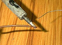
SOLDERING IRONS :

Soldering iron is used during soldering process to supply sufficient heat to melt solder by transfer of heat from soldering iron tip. The tip of the soldering iron is applied to a connection which is to be soldered
.
There are generally three classes or types of soldering irons:
1. Resistive soldering irons.

2. Soldering gun.
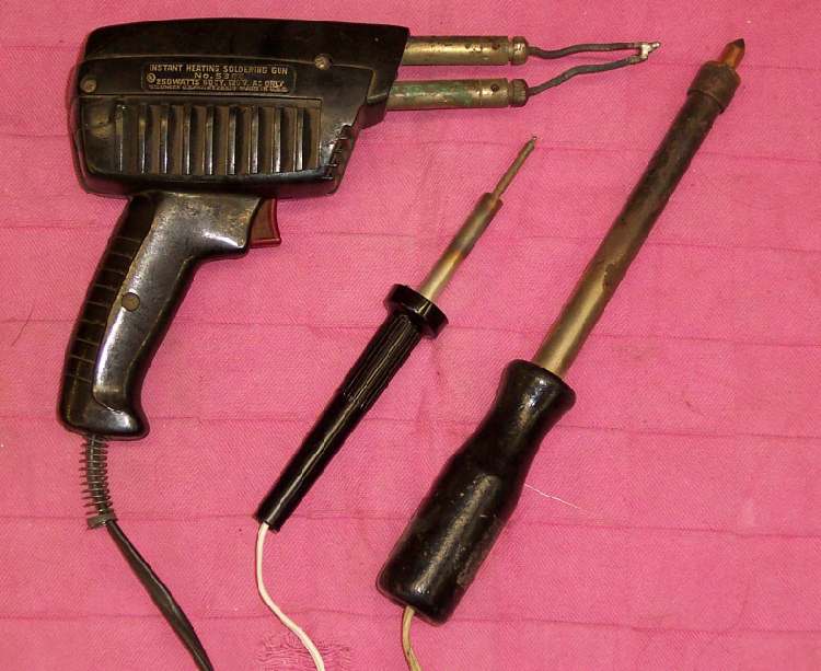
3. Temperature controlled soldering gun.

RESISTIVE SOLDERING IRON:
It is cheapest soldering iron. These can not be used for precision work as heat produced is in excess then required to melt solder. The excessive heat can be very damaging PCB,S and semiconductor devices. This should be used in emergency and when used should be applied for minimum of time to prevent damage of devices due to overheating.
This consists of a copper tip which is heated electrically by resistive coil. This tip acts a heat store and heat conductor.
SOLDERING GUN
Soldering gun is used for soldering heavy wiring. It is not recommended for use on PCB’S. This operates on the principle of resistive heating of low resistance copper tip. Heavy currents flow through the copper tip. Because of the current involved corrosion of attachments nut will result in slow or no heating of the tip. It has trigger switch to control the application of the a.c. power to resistive element. The working Temperature s reached instantaneously.
TEMPERATURE CONTROLLED SOLDERING GUN
The soldering irons are most suited to maintenance purposes especially when dealing with semiconductors components which are likely to be damaged by overheating. This iron operates much slowly as compared to uncontrolled iron.
SELECTION OF SOLDERIONG IRON :
Soldering irons are available in variety of sizes, shapes and wattages. In standard iron, the input voltage is fixed; this resulting temperature depends on capacity of the heating unit and size of the tip. Generally, soldering irons are selected on the basis of the input wattage or the tip, idling, temperature neither of these is valid criterion for matching the right to iron to the job. Ideal tip working temperature is defined as the temperature range between appox 600 to 700 for most electronic assembly.
SOLDERING IRON TIP CLEANING :
Iron plated tips should be cleaned while hot with metal brush or with cellulose sponge (wet) and while cold with a wire brush to remove oxide film. These should not be cleaned with files, sand paper or emery cloth.
DESOLDERING:
This operation is frequently required during maintenance for replacing a component. It consists of removal of solder from a previously soldered joint.
The following techniques are often used for this purpose.
1. USE OF DESOLDERING PUMP
Desoldering pump is a mechanically operated, hand held desoldering tool,. This tool consist of a outer shaft, piston handle and release pin and Teflon pin. It is designed to be held and operated in one hand. The pump can be disassembled and cleaned as required
.
The step by step procedure for desoldering is:
• Load the pump
• Heat the solder connected with soldering iron until solder melts.
• Hold desoldering pump lightly against the melted solder.
• Press the pin to vacuum solder from connection.
• Reload and repeat as necessary to clean the area of solder.
2. USE OF DESOLDERING BRAID
Desoldering braid is loosely woven, flux impregnated, stranded braid of copper wire. The joint to be desoldered is not heated using soldering iron. The braid (wick) is heated first. The solder is sucked into the braid due to capillary action when it is brought near joint. The used portion is cut and thrown away. In this method soldering iron never touches the solder so prevents over heating of components.
3. USE OF DESOLDERING BULB
This also operates on vacuum principle. The rubber is simply a hollow rubber ball with heat resistant Teflon tip. It can be used with any soldering iron.
The iron is held in one hand and used to melt the solder. The bulb held in second hand is then squeezed to create vacuum. The tip is next applied to the reheated solder. Connection action that sucks the solder up through hollow tip into bulb.
4. USE OF DESOLDERING TIP AND DIP EXTRACTOR
This method is used for desoldering IC’S. Here clips of the extractor are fixed over the chip and DIP chip is applied at the other side of the PCB. All connection will melt simultaneously. As the extractor is spring loaded , the IC chip will automatically come up once the solder melts.
SOLDERING DEFECTS:
The defects can be classified according to their nature into major or minor defects.
Some of the defects encountered during soldering are:
DEWETTING- It occurs due to contaminated base metal surface. Dewetting of solder film as water on greasy surface.
PARTIAL WETTING- This is due to incomplete coverage of the surface by solder film. This is usually a result of an inadequate time temperature cycle or of insufficient flux activity.
OTHER SOLDERING DEFECTS MAY OCCUR DURING SOLDERING PROCESS ARE:
• EXCESS SOLDER
• ICICLES
• BRIDGING
• POROSITY
• OVER HEATED JOINTS
COMPONENT PREPRATION AND MOUNTING.
Components are generally on one side of PCB. In double sided PCB’s, the component are generally mounted usually opposite to the major conductor pattern side depending upon design.
Before mounting any component it is essential to clean the surface to be soldered with some braided cleaning tool. Component leads are bent so that component properly fit into the circuit. Bending of component should be done with minimum stress. The bent leads should fit into the holes perpendicular to the board
.
• Horizontally mounted components should touch the board surface to avoid lifting of solder joint.
• Vertically mounted components should not be flush to the board to avoid strain on solder joint.
• Sealed components should be mounted in such a way to provide a certain distance from the board as insulation coating on component is extended to a certain length along the leads.

Like it on Facebook, Tweet it or share this article on other bookmarking websites.